Cold Solder Joint vs. Good Solder Joint

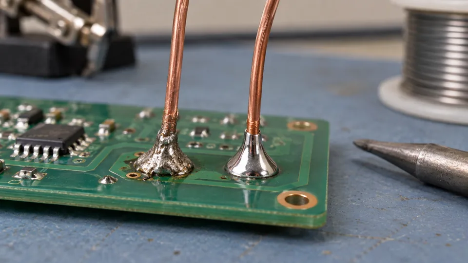
A cold solder joint forms when solder fails to wet and bond properly to the surfaces being joined. Insufficient heat is a common cause, but contamination, inadequate flux, poor tip contact, and movement during cooling can produce similar defects. A good solder joint has complete wetting, an appropriate solder volume, stable alignment, and no visible cracks, gaps, or unintended bridges.
Brightness is a weak basis for comparison. Some acceptable joints are shiny, while others appear matte because of the solder alloy or process. Inspect the joint’s shape, wetting boundaries, coverage, and mechanical stability instead.
Cold Solder Joint vs. Good Solder Joint at a Glance
| Characteristic | Cold or Defective Joint | Good Joint |
|---|---|---|
| Wetting | Solder may sit on the lead, pad, terminal, or wire as a bead with a distinct boundary or visible gap | Solder spreads onto the required surfaces and transitions smoothly into them |
| Shape | Irregular, lumpy, peaked, or poorly formed | Consistent with the joint geometry, often forming a smooth fillet |
| Surface | May look rough, grainy, cracked, or disturbed | Generally uniform for the alloy and process used |
| Mechanical condition | Lead, wire, or terminal may move within the solder, or the joint may contain a circumferential crack | Joined parts remain stable without relying on a loose solder shell |
| Electrical behavior | May have excessive resistance, intermittent continuity, or failure under vibration or temperature changes | Provides a stable electrical connection appropriate for the circuit |
| Typical causes | Poor heat transfer, dirty surfaces, depleted flux, movement during cooling, or incompatible materials | Clean solderable surfaces, effective flux, proper heating, adequate wetting, and undisturbed cooling |
What a Cold Solder Joint Actually Is
The term cold solder joint is often applied broadly to any joint that looks rough or performs intermittently. More precisely, it describes a connection in which the soldering process did not create satisfactory wetting and bonding. The solder may have melted without bringing the lead, pad, terminal, or wire surface to the condition needed for proper wetting.
Melting solder directly on the iron and depositing it onto a cool connection is a common way to create this problem. Molten solder can cover the joint while failing to bond adequately beneath the visible surface.
Movement during solidification can create a disturbed or fractured joint that looks similar and may produce the same electrical symptoms. Technicians sometimes group these defects under the cold-joint label, although their immediate causes differ.
How to Identify a Good Solder Joint
A satisfactory joint should be evaluated in relation to its construction. A through-hole lead, an SMD termination, a wire splice, and a connector lug do not share one ideal shape. Several characteristics remain useful across these applications.
Clear wetting to both surfaces
Solder should flow onto each surface that must be joined. On a through-hole connection, that usually means the component lead and the exposed land around the hole. On an SMD joint, the solder should wet the component termination and the PCB pad. Wire and terminal joints require wetting to the intended conductors or lug surfaces.
Poorly wetted solder often forms a rounded bead with an abrupt edge. A properly wetted fillet usually tapers toward the joined surfaces rather than appearing to rest on top of them.
An appropriate amount of solder
More solder does not guarantee a stronger or more conductive connection. Excess solder can conceal incomplete wetting, cracks, component alignment problems, and bridges to nearby conductors. Too little solder may leave required surfaces incompletely covered or fail to form the intended connection.
The component outline and joint boundaries should remain inspectable where the assembly geometry permits. Large blobs that obscure the lead and pad deserve closer examination.
No signs of movement or damage
A good joint should have no visible crack around the lead or terminal. It should also be free from lifted pads, scorched board material, melted insulation, damaged component bodies, or separated traces. These conditions are separate from a cold joint, but they can result from unsuccessful or repeated rework.
A surface consistent with the solder alloy
Traditional tin-lead solder commonly produces a reflective surface under suitable conditions. Many lead-free alloys can form acceptable joints with a less reflective or slightly textured finish. Oxidation, solidification behavior, and the joint geometry also affect appearance.
A very rough, frosted, or fractured surface can support a diagnosis when combined with poor wetting or instability. A matte finish by itself is insufficient evidence of a defect.
Warning Signs and What They May Indicate
| Observation | Possible Explanation | Next Check |
|---|---|---|
| Solder forms a ball on the pad or lead | Contamination, oxidation, inadequate flux, or insufficient heating of the work | Check surface cleanliness, solderability, flux condition, and whether the tip contacts both joined parts |
| Joint has an irregular or grainy surface | Movement during cooling, poor wetting, alloy characteristics, or an unstable heating process | Inspect for cracks, visible gaps, and movement rather than judging texture alone |
| Circular crack appears around a component lead | Mechanical stress, thermal cycling, disturbed solidification, or a degraded original joint | Check component support and inspect the pad for lifting or trace damage before rework |
| Solder wets the pad but pulls away from the lead | Oxidized, contaminated, plated, or otherwise difficult-to-solder lead | Confirm that the lead is clean and intended to be soldered with the chosen flux and solder |
| Solder wets the lead but does not spread across the pad | Poor heat transfer into the land, contaminated copper, damaged plating, or insufficient flux | Inspect the land and use a tip geometry that provides useful contact without touching nearby parts |
| Connection works when pressed or flexed | Cracked joint, loose conductor, damaged trace, connector fault, or another intermittent path | Disconnect power and inspect the full connection area under magnification |
| Joint is a large smooth blob | Excess solder may be hiding poor wetting | Look for a visible transition into both surfaces and remove excess solder if inspection is blocked |
Why Cold Joints Form
Weak heat transfer into the connection
The iron must transfer heat into the parts being joined. A tiny tip can struggle with a large pad, connector terminal, heavy wire, or ground plane because it provides little contact area and has limited thermal coupling. Raising the temperature setting may still produce slow, uneven heating while increasing the chance of damaging nearby materials.
A compatible tip with suitable geometry and adequate contact area often transfers heat more effectively. The best choice must still fit the available space and avoid adjacent components.
The tip heats only one side
Touching the iron to the component lead while barely contacting the pad, or heating the pad without reaching the lead, can leave one surface too cool for wetting. Position the tip so it makes useful thermal contact with both parts where the joint geometry allows.
Dirty or oxidized surfaces
Oxides, oils, old residue, corrosion, and damaged plating can prevent molten solder from spreading. Flux helps remove manageable surface oxides during heating, but it cannot restore every corroded lead or damaged PCB land. Materials that remain unwettable after careful cleaning and a controlled attempt may require replacement or repair rather than repeated heating.
Flux is absent, exhausted, or unsuitable
Flux chemistry must suit the soldering process and the materials. Old solder on a joint may contain little active flux after its original heating cycle. Adding compatible flux before reflow often improves wetting, while simply melting the old solder may reproduce the defect.
The connection moves while cooling
Solder needs to solidify without movement between the joined parts. An unsecured wire, loose connector pin, or component lead under tension can shift during cooling and disturb the joint. Solder should not serve as the sole strain relief for wiring exposed to pulling, bending, or vibration.
How to Repair a Suspected Cold Solder Joint
-
Disconnect power and inspect the area. Remove batteries and other energy sources where applicable. Use adequate lighting and magnification to check for cracks, bridges, lifted pads, loose terminals, damaged insulation, and contamination.
-
Stabilize the parts. Secure a moving wire or component so the connection will remain still while the solder solidifies. Correct mechanical strain before reflowing the joint.
-
Apply compatible flux. A small amount of suitable electronics flux can help the existing solder reflow and wet the surfaces. Confirm compatibility with the solder alloy, board, component, and cleaning process.
-
Use a clean, tinned tip with useful contact area. Select a tip that reaches the joint and contacts the relevant surfaces effectively. A small chisel or bevel may provide better heat transfer than a needle-like tip in many PCB applications, provided there is enough clearance.
-
Heat the joined surfaces together. Place the tip against the lead and pad, wire and terminal, or other mating surfaces. Avoid hard pressure. The goal is efficient thermal contact, not scraping.
-
Allow the solder to flow and wet. Add a modest amount of compatible solder if fresh solder and flux are needed. Feed it at the heated joint rather than coating the iron and carrying a blob across. Watch for the solder to spread into the surfaces.
-
Remove excess or contaminated solder when necessary. If a large blob prevents inspection, the solder is heavily oxidized, or contamination is present, use suitable desoldering braid or another controlled removal method. Then rebuild the joint with fresh flux and solder.
-
Let the connection cool without movement. Remove the solder feed first, then withdraw the iron while keeping the assembly stable. Do not blow on or disturb the joint.
-
Inspect and test. Confirm wetting, clearance from adjacent conductors, alignment, and the absence of cracks or damage. Clean residue where the flux chemistry or assembly requirements call for cleaning.
Temperature settings depend on the alloy, joint size, copper area, tip, station behavior, and component limits. If solder remains unwilling to wet, stop and identify the cause rather than repeatedly increasing heat or extending contact. Persistent trouble may indicate an unsuitable tip, contaminated surface, incompatible materials, damaged plating, or inadequate equipment for the joint’s thermal demand.
Verification Beyond Appearance
Visual inspection is the first check, not a complete guarantee. A connection can look smooth while hiding poor wetting beneath excess solder. It can also pass a simple continuity check yet become intermittent under normal mechanical or thermal conditions.
- Magnified inspection: Look at the entire boundary between the solder and each joined surface. Check neighboring pads for bridges and solder debris.
- Mechanical inspection: Confirm that the component, terminal, or wire is properly supported. Avoid forceful probing that could tear a pad or create a new crack.
- Electrical testing: With the circuit safely unpowered, continuity or resistance measurements may reveal an open or unstable connection. Parallel circuit paths can complicate readings.
- Functional testing: Power the assembly under appropriate controlled conditions after inspection. A remaining fault may originate elsewhere in the circuit rather than at the repaired joint.
If a pad starts lifting, a trace separates, insulation recedes, or the component body shows heat damage, further reflow can make the repair harder. Stop heating and assess whether the board needs trace repair, pad repair, wire reinforcement, or component replacement.

- Jesse
Jesse is the editor behind Soldering Gear, where he covers soldering irons, stations, rework equipment, and the tools that belong on a practical electronics bench. His work focuses on comparing product specifications, features, compatibility, and intended uses so readers can make more informed buying decisions.
- Best Soldering Iron for Microsoldering: 9 Picks in 2026 November 10, 2026
- Best Soldering Station for PCB Repair: 9 Picks in 2026 November 9, 2026
- How to Desolder Electronics November 8, 2026
- Best Hot Air Rework Station for PCB Repair: 9 Picks in 2026 November 7, 2026
- Soldering Iron Tip Shapes Explained November 6, 2026