Soldering Iron Tip Shapes Explained

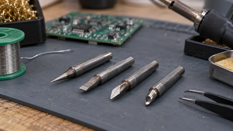
A soldering iron tip’s shape determines how much of the heated surface can touch a joint, which angles are practical, and how easily solder can be controlled. A tiny pointed tip offers excellent access but often transfers heat poorly. A wider chisel or bevel can heat the same small pad more efficiently because it creates a larger contact area.
Choosing a tip is therefore a question of joint geometry, thermal demand, and access. Component size matters, but the smallest component does not automatically call for the finest available point.
How tip shape affects soldering
Heat passes from the tip into the lead, pad, terminal, or wire through the area where their surfaces meet. A broad, well-tinned contact face usually transfers heat faster than a narrow point making marginal contact. Faster transfer can shorten the time the iron must remain on the joint, provided the tip is appropriately sized and the temperature setting suits the solder and workpiece.
Three characteristics are especially useful when comparing tip shapes:
- Contact area: A larger contact patch generally delivers heat more effectively to a joint with significant thermal mass.
- Access: Narrow or angled tips can reach between components and into restricted locations.
- Solder control: Flat, beveled, concave, and blade-shaped faces can hold or guide different amounts of molten solder.
The tip must also fit the physical scale of the work. A face that overlaps nearby pads can create bridges or touch adjacent components. A face that is far smaller than the joint may struggle to maintain working temperature at the contact point.
Common soldering iron tip shapes explained
| Tip shape | Main characteristic | Common applications | Main limitation |
|---|---|---|---|
| Conical | Tapered body ending in a rounded point | General electronics, confined joints, light touch-up work | The point provides limited contact area |
| Needle or extra-fine conical | Very narrow, elongated point | Restricted access and very small exposed features | Low heat-transfer capacity at the extreme tip |
| Chisel | Flat working face with defined width | Through-hole joints, wires, terminals, many SMD pads | A wide version may obstruct access or contact adjacent features |
| Screwdriver | Broad flat edge, often similar to a heavy chisel | Larger terminals, connectors, wire work, substantial joints | Usually too large for crowded fine work |
| Bevel | Angled circular or oval face | General PCB work, larger pads, solder feeding, drag techniques | Orientation and solder quantity require control |
| Hoof or concave bevel | Angled face with a shallow solder reservoir | Drag soldering and work requiring a controlled solder film | Can deposit excessive solder if overloaded |
| Knife or blade | Thin blade with an edge and broad side surfaces | Drag soldering, bridge removal, rows of leads, tight access | The edge can be awkward on isolated round joints |
| Bent or angled | Working end offset from the tip’s main axis | Joints hidden behind components or beneath overhangs | Less intuitive positioning and more limited general use |
Manufacturers do not use these names with complete consistency. A tip called a bevel by one company may resemble another company’s hoof tip. Dimensions, face geometry, plating, and tip-series compatibility provide more reliable information than the shape name by itself.
Conical tips
A conical tip tapers evenly toward a rounded point. It is commonly supplied with basic soldering irons because it can approach a joint from several directions and fits into crowded spaces.
The narrow end is useful where access is the main constraint, but it has little surface area. Operators sometimes respond by raising the temperature or pressing harder. Neither approach fixes poor geometric contact. Excessive pressure can damage tip plating or the workpiece, while excess heat can increase the risk of damaged pads, degraded flux, and shortened tip life.
A conical tip does not have to touch a joint with its absolute point. Depending on its construction and the available space, placing the tapered side against both the pad and lead can create better thermal contact. A small amount of fresh solder at the interface also helps bridge microscopic gaps between the surfaces.
Needle tips
Needle tips are longer and finer than ordinary conical tips. Their appearance suggests precision, but their thermal performance at the point is limited. They can be useful for reaching a tiny exposed area surrounded by obstructions. For routine small-component soldering, a compact chisel often provides better heat transfer while retaining adequate control.
Chisel and screwdriver tips
A chisel tip has a flat face and two usable corners. Rotating the iron changes the contact geometry: the broad face can heat a pad and lead together, while a corner can reach a smaller feature. This versatility makes the chisel one of the most practical shapes for general electronics work.
Small chisels work well for many surface-mount and through-hole joints. Medium or large versions suit heavier leads, wires, connector tabs, ground pads, and other thermally demanding work. The useful dimension is the width of the face relative to the joint, nearby conductors, and available clearance.
A screwdriver tip follows the same basic principle but is often broader or heavier. Terminology varies, and some catalogs use “chisel” and “screwdriver” for nearly identical profiles. Both rely on a flat working surface rather than a point.
Why a chisel can outperform a fine point
Consider a small through-hole joint connected to a broad copper area. A needle tip may fit easily, yet touch only a tiny part of the lead and pad. A modest chisel can contact both surfaces over a larger area and replenish heat more effectively as the copper draws energy away. The chisel may complete the joint with less dwell time without requiring a higher temperature setting.
The chisel should still fit within the workspace. If its face reaches neighboring pads or plastic housings, a narrower version or a different orientation is appropriate.
Bevel and hoof tips
A bevel tip ends in an angled face, usually circular or oval. The face provides a useful contact area, and its angle lets the operator place molten solder where it is needed. Bevels are suitable for larger pads, wires, through-hole work, and some surface-mount techniques.
Some bevel tips have a flat angled face. Others have a shallow cavity and are commonly called hoof, spoon, or concave tips. The cavity retains a small solder reservoir. During drag soldering, that reservoir can carry a film of solder across a row of fluxed leads.
Reservoir capacity is helpful only while the solder quantity remains controlled. An overloaded hoof tip can leave bridges between adjacent leads. Flux, board orientation, tip movement, pad condition, and lead spacing also affect the result. Fine-pitch packages may be better handled with another process, such as solder paste and reflow or hot air, depending on the package and repair context.
Knife and blade tips
A knife tip resembles a narrow blade. Its edge can fit between closely spaced features, while either side provides more thermal contact than the edge alone. The long working surface is useful for heating a row of leads, moving across several pads, or addressing a solder bridge.
For drag soldering, the blade can carry a controlled film along fluxed leads. For bridge correction, a clean, properly tinned blade may help draw molten solder away from the affected area. Solder wick is often more predictable where a larger amount must be removed.
Blade tips require careful orientation. The pointed end can concentrate contact in a small area, while the broad side may span several conductors. Nearby plastic parts, solder mask condition, and component clearance should guide the approach angle.
Bent and specialty profiles
A bent tip offsets the working end from the handpiece axis. The offset improves visibility or access around tall components, shields, connector bodies, and overhanging parts. Bent tips may use conical, chisel, or bevel working faces, so “bent” describes the tip’s orientation rather than its contact geometry.
Other specialty profiles include tunnel tips for certain integrated-circuit packages, spatula tips for broad contact areas, and extra-heavy tips for large conductors or metalwork. Their usefulness depends on a close match between the working face and the intended joint. They are less adaptable than common chisel or bevel profiles.
Matching the tip to the joint
Tip selection is easier when the joint is evaluated as a physical contact problem rather than by component category alone. Examine the surfaces that must be heated together and the obstacles surrounding them.
- Identify the heated surfaces. A sound soldering approach usually requires contact with both parts of the joint, such as a component lead and PCB pad or two prepared wire surfaces.
- Estimate the thermal demand. Thick leads, large terminals, heavy wires, broad copper pours, and multilayer ground connections may draw heat away quickly.
- Check the available clearance. Account for adjacent pads, component bodies, insulation, plastic connectors, and board edges.
- Choose the largest practical contact face. The face should make effective contact without touching areas that must remain undisturbed.
- Plan the approach angle. Chisel corners, bevel faces, and knife edges behave differently as the handpiece is rotated.
Through-hole PCB joints
A small or medium chisel is a useful starting point for many through-hole joints because its face can touch the pad and lead at the same time. A conical tip may work where access is tight. Ground connections and large plated holes can require a broader face with greater heat-transfer capacity.
Surface-mount components
Small chisels are effective for many individual chip-component pads and gull-wing leads. Hoof and knife tips can suit drag soldering across rows of leads. Very fine conical tips make sense where clearance prevents a broader face from reaching the exposed metal, but they should not be selected solely because the component is small.
Wires and terminals
Wire joints and connector tabs usually benefit from a chisel, screwdriver, or bevel with enough area to transfer heat into both surfaces. A narrow point may melt solder on itself while the wire or terminal remains too cool for proper wetting. Connections exposed to pulling or repeated movement also need suitable mechanical support or strain relief. Solder should not serve as the sole structural support in those situations.
Large copper areas
Ground planes, shields, heavy conductors, and large lugs can absorb heat rapidly. A broad chisel or bevel is generally more suitable than a needle tip. If a correctly sized tip and appropriate technique still cannot heat the joint effectively, the iron or station may lack the necessary thermal capacity. Raising the setting repeatedly is a poor substitute for suitable equipment and contact geometry.
Tip size, temperature, and thermal recovery
Shape cannot be separated completely from tip size and iron performance. Two chisel tips with the same nominal width may behave differently if their construction, heater coupling, mass, or plating differs. Cartridge tips, internally heated tips, and traditional slip-on tips also transfer and recover heat differently.
The selected temperature depends on the solder alloy, flux, workpiece, tip, station behavior, and component limitations. Changing from a needle to a suitable chisel may improve heat delivery enough that a higher setting is unnecessary. Fresh solder on the working face helps establish contact, but a large blob is not a replacement for the correct tip.
If solder melts on the tip yet refuses to wet the joint, check the following before increasing heat:
- Whether the working face is clean, tinned, and wettable
- Whether the tip is touching both parts of the joint
- Whether oxidation or contamination is preventing wetting
- Whether suitable flux is present
- Whether the tip face is too small for the joint’s thermal demand
- Whether the equipment can maintain useful tip temperature under load
Stop and reassess if extended heating causes pad movement, board discoloration, softening insulation, or damage to nearby components. Repeated reheating can make a repair harder rather than correcting the underlying contact or preparation problem.
Tip compatibility and manufacturer naming
Replacement tips are not universally interchangeable. The shape may look correct while the heater interface, length, sensor arrangement, diameter, locking method, or calibration requirements differ. Tips must match the soldering iron, handpiece, or cartridge family specified for the equipment.
Catalog codes also vary. Letters such as B, C, D, I, J, K, or BC may identify shapes within one manufacturer’s system, but those codes do not have a universal meaning. Confirm the following before selecting a replacement:
- The compatible iron or handpiece series
- The manufacturer’s dimension drawing
- The width or diameter of the working face
- Whether the face is flat, angled, concave, pointed, or bladed
- The overall reach and any bend or offset
Preserving the working shape
Modern electronics tips commonly have a plated working surface over a copper core. Filing, grinding, or aggressive abrasion can breach that plating and expose the copper, leading to rapid erosion. Routine care should rely on compatible cleaning methods, suitable tip cleaner where needed, and a protective solder coating.
Keep the working face tinned during use and leave a coating of solder on it before switching off the iron. If a tip no longer wets after appropriate cleaning and re-tinning attempts, or if its plating is visibly breached, replacement is usually more practical than reshaping it.
A compact set covering a small chisel, a medium chisel or bevel, and one access-oriented shape handles many electronics tasks. The best choice for any particular joint is the shape that reaches safely, contacts the required surfaces, and transfers heat efficiently without crowding adjacent features.

- Jesse
Jesse is the editor behind Soldering Gear, where he covers soldering irons, stations, rework equipment, and the tools that belong on a practical electronics bench. His work focuses on comparing product specifications, features, compatibility, and intended uses so readers can make more informed buying decisions.
- Best Soldering Iron for Microsoldering: 9 Picks in 2026 November 10, 2026
- Best Soldering Station for PCB Repair: 9 Picks in 2026 November 9, 2026
- How to Desolder Electronics November 8, 2026
- Best Hot Air Rework Station for PCB Repair: 9 Picks in 2026 November 7, 2026
- Soldering Iron Tip Shapes Explained November 6, 2026