How to Solder Through-Hole Components

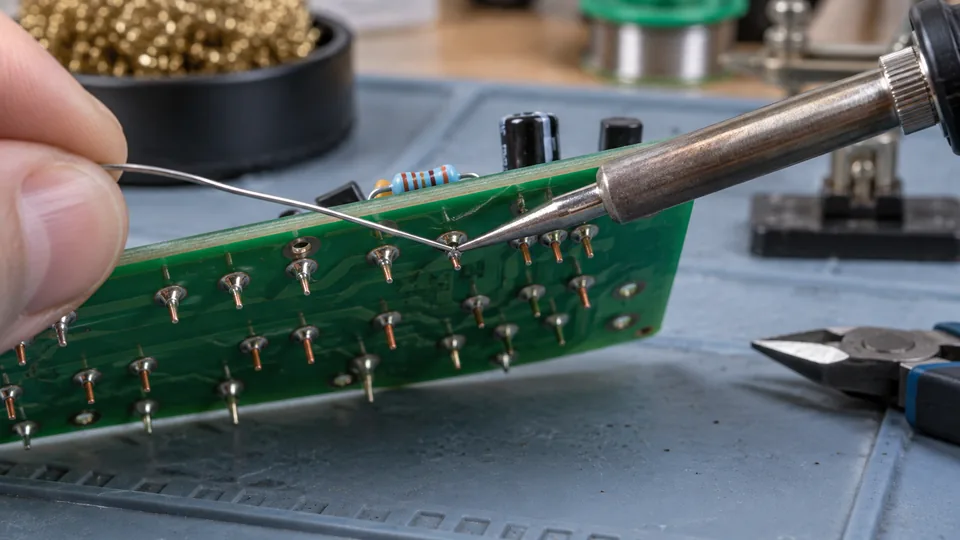
A reliable through-hole joint forms when the component lead and copper pad reach soldering temperature together. Solder should wet both surfaces and create a continuous bond around the lead. Melting solder onto the iron first and transferring it to a cool joint often produces poor wetting, excess solder, or an unstable connection.
Learning how to solder through-hole components is largely a matter of controlling contact, heat transfer, solder quantity, and movement. Preparation matters because oxidation, incorrect component placement, or a poorly chosen tip can undermine otherwise careful technique.
Prepare the board and components
Confirm component values, locations, and orientation before heating the board. Resistors and many ceramic capacitors are electrically nonpolarized, but orientation may still be specified for consistent labeling. LEDs, diodes, electrolytic capacitors, transistors, integrated circuits, and some connectors must face the correct direction.
Use the PCB markings, schematic, assembly drawing, and component datasheet where needed. Polarity indicators vary between component types, so avoid relying on one marking convention for every part.
Insert each component without forcing its leads through the holes. For axial components, form bends a short distance from the body rather than sharply bending the lead where it enters the package. A lead-forming tool can produce consistent spacing and reduce stress on the component.
Seat the part as required by the board design. Some components sit close to the PCB, while power resistors and other heat-producing parts may require clearance. Connectors, switches, and sockets should sit squarely against their intended mounting surface.
Slightly spreading or bending the leads on the solder side can hold a component in place. Avoid flattening them tightly against the board. Severe bends make trimming and later replacement more difficult, and they can place unnecessary stress on the pad.
Select equipment that can heat the joint effectively
A temperature-controlled soldering iron, suitable solder, a stable iron stand, and flush or semi-flush cutters cover most through-hole assembly work. Flux-cored electronics solder is commonly used. Additional compatible flux can help with oxidized surfaces or rework, but it should match the soldering process and any cleaning requirements.
Choose a tip that can touch the lead and pad at the same time. A small chisel or bevel tip often provides better contact than a needle-like tip. Tip access, pad size, lead diameter, nearby parts, and the copper area connected to the pad all influence the best geometry.
The correct station setting depends on the solder alloy, tip, board construction, joint size, and iron behavior. Follow relevant solder and equipment guidance. If a joint heats slowly, first check tip condition, contact area, and thermal demand rather than immediately raising the temperature.
Keep the work supported so it cannot slide while the solder cools. Good lighting helps reveal pad edges, bridges, and component markings. Magnification is useful for closely spaced pins but is rarely necessary for every large through-hole joint.
Solder the through-hole joint
-
Clean and tin the iron tip. Wipe the hot tip using the cleaning method appropriate for the equipment, then apply a small amount of fresh solder. A thin solder coating protects the working surface and improves thermal contact. The tip should be wetted rather than carrying a large hanging blob.
-
Place the tip against both surfaces. Touch the working face of the tip to the component lead and copper pad simultaneously. Use light contact. Pressing hard does little to improve heat transfer and may damage the pad or tip.
-
Feed solder into the heated joint. Apply solder where the lead and pad meet, preferably from the side opposite the iron. The hot surfaces should melt the solder. Feeding a small initial amount near the tip can establish a thermal bridge, after which the solder should flow around the joint.
-
Stop adding solder once the joint is covered. The solder should wet the lead and pad without hiding the entire pad beneath a rounded mass. The required quantity varies with pad and lead geometry. More solder does not compensate for poor wetting.
-
Remove the solder wire, then remove the iron. Keeping this sequence prevents the solder wire from freezing into the joint. Once the iron is lifted, hold the board and component still while the solder solidifies.
-
Trim the lead safely. Cut the excess lead just above the completed joint without cutting into the solder fillet or stressing the pad. Hold or shield the loose end so it cannot fly toward your face or nearby equipment. Eye protection is useful during trimming.
Work at a steady pace, but do not use a rigid time limit for every connection. A small resistor lead on a light copper pad heats differently from a connector pin attached to a ground plane. Watch how the solder responds. If it does not begin wetting normally, remove the iron and reassess rather than continuing to heat the same spot.
Recognize a satisfactory joint
A sound through-hole joint usually shows continuous wetting between the solder, component lead, and copper pad. Its outline should make the relationship between those surfaces visible instead of resembling a loose ball sitting on top of the pad.
Look for these practical indicators:
- The solder has flowed around the lead rather than clinging to one side.
- The pad and lead show a continuous bonded area without obvious cracks or gaps.
- The component did not move as the joint cooled.
- No solder connects neighboring pads that should remain separate.
- The pad remains attached and shows no signs of lifting or trace damage.
- The amount of solder is sufficient for coverage without obscuring adjacent features.
Surface brightness varies with alloy, cooling behavior, and process conditions. A dull joint is not automatically defective, and a reflective joint is not guaranteed to be sound. Wetting, continuity of the bond, component stability, and the absence of damage provide more useful evidence.
For plated through-holes, solder may be visible on both sides of the board when the hole and process allow it. Required barrel fill depends on the board, accessibility, and applicable assembly criteria. Do not keep heating a finished joint solely to chase an appearance that the particular board cannot readily produce.
Adjust the technique for demanding components
Connectors, sockets, and multi-pin parts
Alignment is easier to correct before every pin is soldered. Solder one pin, check that the part is fully seated and square, then solder a pin near the opposite end. If adjustment is needed, reheat the first joint carefully while repositioning the part without levering against the pad.
After alignment is confirmed, complete the remaining pins. Inspect between adjacent pins for bridges, especially where the pads are closely spaced.
Ground planes and large leads
Pads connected to broad copper areas draw heat away from the joint. A tip with greater contact area can transfer heat more efficiently than a very fine tip at a higher setting. Large connector tabs, terminal posts, and heavy leads may also require equipment with enough thermal capacity for the joint.
If the solder melts on the tip but beads on the pad, the pad may still be too cool, contaminated, or oxidized. Check the surface, flux, tip fit, and equipment capability before applying prolonged heat.
Heat-sensitive and polarized parts
Verify LED, diode, electrolytic capacitor, transistor, and integrated-circuit orientation before soldering. Keep each heating cycle controlled and allow the area to cool before attempting repeated correction. Component datasheets or assembly documentation may specify handling or temperature limits.
Sockets can reduce direct soldering exposure for some integrated circuits, provided a socket is suitable for the design. They also make later replacement easier, although they add another set of electrical contacts.
Single-sided boards
Unplated pads on single-sided boards may have less mechanical support than plated through-holes. Avoid pulling sideways on the lead, reheating repeatedly, or using the iron as a lever. If a pad starts lifting, stop and assess the connection before further work causes trace separation.
Correct common joint problems
| What you see | Likely factors | Practical correction |
|---|---|---|
| Solder forms a ball on the lead or pad | The surfaces may be cool, oxidized, dirty, or lacking suitable flux | Let the area cool, clean it where appropriate, apply compatible flux, and reflow while heating the lead and pad together |
| Solder stays on the tip instead of flowing into the joint | Poor tip placement, inadequate contact area, or contamination may be limiting heat transfer | Clean and retin the tip, use a better-fitting tip geometry, and contact both joint surfaces |
| Joint has a cracked or irregular surface | The component or board may have moved during cooling | Stabilize the assembly, add flux if appropriate, and reflow the joint once with controlled heat |
| Large rounded mound hides the lead and pad | Too much solder was applied, possibly without full wetting underneath | Remove excess with solder wick or another suitable desoldering method, then inspect and reflow if needed |
| Solder joins adjacent pads | Excess solder, poor tip control, or close spacing produced a bridge | Apply compatible flux and draw away the excess with a clean tip or solder wick, then inspect between the pins |
| Pad begins to discolor, loosen, or lift | Repeated heating, excessive contact time, force, or prior damage may be involved | Stop heating and allow the area to cool. Assess whether the pad and trace remain intact before attempting a repair |
Rework should be deliberate. Repeatedly melting the same connection can weaken pad adhesion, damage the through-hole plating, or overheat the component. If one careful reflow does not solve the problem, check for contaminated surfaces, an unsuitable tip, insufficient thermal capacity, damaged copper, or incompatible materials.
Inspect and test before applying power
Examine the component side for orientation, seating, and accidental lead contact. On the solder side, check every intended joint and scan neighboring pads for bridges, clipped lead fragments, and solder splashes. Confirm that trimmed leads cannot touch an enclosure, another trace, or conductive hardware.
Electrical checks should match the circuit. A multimeter can help identify unintended shorts across supply rails, verify selected connections, or confirm that polarized parts are installed correctly. Circuit paths through other components can affect continuity readings, so interpret them using the schematic rather than treating every beep as a definitive result.
Keep the iron in a stable stand, work away from flammable clutter, and manage flux fumes with ventilation appropriate for the workspace and process. Flux generates much of the visible smoke during ordinary electronics soldering. Solder containing lead calls for careful handling, clean work surfaces, and hand washing after use, especially before eating or touching the face.

- Jesse
Jesse is the editor behind Soldering Gear, where he covers soldering irons, stations, rework equipment, and the tools that belong on a practical electronics bench. His work focuses on comparing product specifications, features, compatibility, and intended uses so readers can make more informed buying decisions.
- Best Soldering Iron for Microsoldering: 9 Picks in 2026 November 10, 2026
- Best Soldering Station for PCB Repair: 9 Picks in 2026 November 9, 2026
- How to Desolder Electronics November 8, 2026
- Best Hot Air Rework Station for PCB Repair: 9 Picks in 2026 November 7, 2026
- Soldering Iron Tip Shapes Explained November 6, 2026